Wikipedia

Search results

Sunday, June 17, 2012

intelligent combat robot ver-02


Intelligent Combat Robot

   We cannot forget 9/11 when 101 people including nine foreigners and 14 policemen have lost their lives while about 300 people were injured in the worst terror attack seen in the country in which desperate men fired indiscriminately at people.Being an ex– defense person , my blood was boiling as our brave soldiers were fighting the militants to free all the hostages from mumbai hotels.


Intelligent Combat Robot Block Diagram

It struck an adea in my mind, why cant we make a robot to tackle such type of situation.
This combat robo is an improved version of my previous robot which I designed years ago named SPY ROBO.
Out new Combat robo is radio operated , it has got two barrel turret through bullet can be fired, radio camera in synchronization with the turret can rotate up and down ,left and right upto a safe firing limit.turret and camera mechanisim has been installed on my previous spy robo vehicle,which has all the function like tank, turing to any angle on its axix, moving forward and reverse turning left and right,running instanty into reverse direction.

This robo is radio operated , self powered , and has all the controls like a normal car. A pair of laser gun has been installed on it, so that it can fire on enemy remotely when required, this is not possible until a wireless camera is installed.

Wireless camera will send real time video and audio signals which could be seen on a remote monitor and action can be taken accordingly. It can silently enter into enemy area and send us all the information through its’ tiny camera eyes. It is designed for, fighting as well as suicide attack.

Heart of our robo is intel’most power family of microcontroller 8051,we are using at89c2051 Two microcontrollers ic2 is first microcontroller which acts as master controller ,decodes all the commands received from the transmitter and give commands to slave microcontroller1 ic3,and slave2 ic5.

Slave microcontrollers are responsible for executing all the commands received from the master and also generating pwm pulses for the speed control . Ic4 is ld293 motor driver ic which drives two nos motors m1 and m2.these two motors are vehicle driver motors.

Slave2 microcontroller controls the gun and camera movements in up/down ,left or right direction. Ic6 is driver ic which drives gun and camera motors in two angles.

Circuit operation receiver:
RF433-RX is 433mhz radio receiver which receives the transmitted codes from the remote place transmitted by the transmitter these codes are converted to digital format and out put is available to the pin no 2 of the ic2 master micro-controller, this is the rx pin of inbuilt UART of the micro-controller. We are using uart to receive our codes at 1200 boud rate.. Based on the input codes master will give command to slave microcontroll ic3 and robo will behave as follows.
a. moves in forward direction
b. moves in reverse direction,
c. speed controls in both the direction
d. it can even turn left or right while moving forward or in reverse direction.
e. Instent reverse or forward running without stopping
f. In case of bump,moves reverse turn left or right and wail for the next instruction .
g. On the spot left or right turn to pass through the nerrow space
h. We have also added head light, back light.and turing lights to left a right . These lights automatically comes on while robo is in Movement.
i. Pin no 7,8,9.11,12,and 13 of the master micro-controller are connected to the slave micro-controller ic3 to give the following command pulses to the slave micro-controller ic3 pin 2,3,6,7,8 and 9,

1.Start/stop
2. Increase speed
3. Increase speed
4. Direction change
5. Turn left
6. Turn right
Slave microcontroller ic3 pins 15,16,17,18,19 are connected to ic4 motor driver ic, pin17 of the slave gives the pulse width modulation pulse which is connected to pin 1 and 9 of ic4 this is EN pin of ic 4 Pin 18 and 19 controlls one motor m1 and pin 15 and 16 of the slave controller controls the m2 motor.

Thursday, June 14, 2012

Remote Data Acquisition Using Wireless - Scada System

Abstract:-

we have developed an integrated wireless SCADA system for monitoring & 
accessing the performance of remotely situated device parameter such as temperature, 
pressure, humidity on real time basis. For this we have used the infrastructure of the existing 
mobile network, which is based on GPRS technique Supervisory Control and Data 
Acquisition (SCADA) is a field of constant development and research. This project 
investigates on creating an extremely low cost device which can be adapted to many 
different SCADA applications via some very basic programming, and plugging in the relevant 
peripherals. Much of the price in some expensive SCADA applications is a result of using 
specialized communication infrastructure. The application of infrastructure, in the proposed 
scheme the cost will come down. Additionally the generic nature of the device will be 
assured. 
 Wireless SCADA deals with the creation of an inexpensive, yet adaptable and easy to use 
SCADA device and infrastructure using the mobile telephone network, in particular, the 
General Packet Radio Service (GPRS). The hardware components making up the device are 
relatively unsophisticated, yet the custom written  software makes it re-programmable over 
the air, and able to provide a given SCADA application with the ability to send and receive 
control and data signals at any non predetermined time. 
GPRS is a packet-based radio service that enables “always on” connections, eliminating 
repetitive and time-consuming dial-up connections.  It will also provide real throughput in 
excess of 40 Kbps, about the same speed as an excellent landline analog modem 
connection. 
 From the wireless SCADA system which is proposed in setup the temperature of around 
30
o
C could be sufficiently recorded from remote location. In the similar manner reading of 
electric energy meter could be read 223 Kilo Watt Hour (KWH) or 223 Unit.  
      The properly designed SCADA system saves time and money by eliminating the need of 
service personal to visit each site for inspection, data collection /logging or make adjustments

Introduction:-

Supervisory Control and Data Acquisition (SCADA) is a process control system that enables a site operator to 
monitor and control processes that are distributed  among various remote sites. A properly designed SCADA 
system saves time and money by eliminating the need for service personnel to visit each site for inspection, 
data collection/logging or make adjustments.  
Supervisory Control and Data Acquisition systems are computers, controllers, instruments; actuators, networks, 
and interfaces that manage the control of automated industrial processes and allow analysis of those systems 
through data collection .They are used in all types of industries, from electrical distribution systems, to food 
processing, to facility security alarms.[7] 
Supervisory control and data acquisition is used to describe a system where both data acquisition and 
supervisory control are performed. Mobile Supervisory Control and Data Acquisition (referred to as Mobile 
SCADA) is the use of SCADA with the mobile phone network being used as the underlying communication 
medium. GSM is a wireless communication technology; most popular today for transmitting data anywhere in 
the world through SMS with the help of mobile phones.[1],[5] 
General Packet Radio Service (GPRS) is chosen as the specific mobile communication protocol to use as it 
provides an always on-line Inter connection without any time based charges. SMS is a globally accepted
wireless service that enables the transmission of alphanumeric messages between mobile subscribers and
external systems such as electronic mail, paging, and voice-mail systems. It is a store and forward way of 
transmitting messages to and from mobiles.[16] 
SMS benefits includes the delivery of notifications and alerts, guaranteed message delivery, reliable and lowcost communication mechanism for concise information, ability to screen messages and return calls in a
selective way and increased subscriber productivity[5]. 

SCADA systems typically are made of four components: 

Master Unit - This is heart of the system and is centrally located under the operator's control. 

Remote Unit - This unit is installed from where the process is actually monitored. It gathers required data about 

the process and sends it to the master unit. 

Communication Mode - This unit transmits signals/data between the master unit and the remote unit. 

Communication mode can be a cable, wireless media, satellite etc. 

Software - The software is an interface between the operator and the units. It allows the operator to visualize and control the functions

SENSOR: RTD Basics:-

1.  Resistance temperature detectors (RTDs) are made of coils or films of metals (usually platinum).      
When heated, the resistance of the metal increases; when cooled, the resistance decreases.  
3.  Resistance varies with Temperature  
4.  Platinum 100 Ohm at 0°C  
5.  Very accurate  
6.  Very stable 

Characterstic of RTD:-

  R  = R0(1+αT0) 
         Where R0     = Resistance at 0
                      α   = Temperature coefficient of resistance  
                    T0    = Temperature in Degree Centigrade

Energy meter Calculation:-

An electric meter or energy meter is a device that  measures the amount of electrical energy supplied to or      
produced by a residence, business or machine. The most common unit of measurement on the electricity meter 
is the kilowatt hour, which is equal to the amount of energy used by a load of one kilowatt over a period of one 
hour, or 3,600,000 joules. general, energy (E) is equivalent to power (P) multiplied by time (t). To determine E in 
kilowatt-hours, P must be expressed in kilowatts and t must be expressed in hours.[8]
                                         E = Pt 
If P and t are not specified in kilowatts and hours respectively, then they must be converted to those units 
before determining E in kilowatt-hours 

IMPLEMENTATION:-

The proposed implementation the system that solves the problem of continuous monitoring of data acquisition 
system with the help of cheap wireless communication.
The basic components of remote monitoring system designed in this paper include sensors, Signal conditioning 
device, AT90S8515 microcontroller, and mobile phone. The sensors i.e. RTD is used to measure remote area 
temperature or energy meter reading. The microcontroller based data logger is fully depends on what is being 
measured. The AT90S8515 is a low-power, high-performance CMOS 8-bit microcontroller with 8K bytes of insystem programmable Flash memory. The microcontroller is to be programmed using C language. 
For Wireless communication. I have used GSM mobile with GPRS services. In this project NOKIA 3310 hand
set is used for GSM communication. Most NOKIA phones have F-Bus connection that can be used to connect a 
phone to microcontroller. This bus will allow us to send and receive SMS messages.

Frame format:-

Total Frame -98 byte (0-97)   
F-Bus Frame Header (6 Byte)
Byte 0: F-Bus Frame ID (0x1E). 
Byte 1: Destination address (0x00) 
Byte 2: Source addresses (0x0C). 
Byte 3: Message Type 0x02 (SMS Handling). 
Byte 4 & 5: Message length.  
SMS Frame Header (18 Byte) 
Byte 6 to 8: Start of SMS Frame Header (0x00, 
0x01, 0x00)  
Byte 9 to 11: Send SMS Message (0x01, 0x02, 
0x00) 
Byte 12: SMS Centre number length. 0x0a is 10 
bytes long.  
Byte 13: SMSC number type(0x81-unknown0x91-
national 
Byte 14 to 23: SMS Centre phone number 
(TPDU) Transfer Protocol Data Unit (5 Byte) 
Byte 24: Message Type (1-sms submit, 0-sms 
deliver) 
Byte 25: Message Reference if SMS Deliver & 
Validity Indicator used  
Byte 26: Protocol ID. (0x00) 
Byte 27: Data Coding Scheme.  
Byte 28: Message Size is 0x22 in hex or 34 bytes 
long in decimal. 
 This is the size of the unpacked message.
Destination’s Phone Number (12 Bytes) 
Byte 29: Destination’s number length. 
Byte 30: Number type 0x91-international, 0xa1-
national  
Byte 31 to 40: (Octet format) Destination’s Phone 
Number 
Validity Period (7 Byte) 
Byte 41: Validity-Period Code. (0xFF) 
Byte 42 to 47: Service Centre Time Stamp (0x00…. 
0x00) 
The SMS Message (SMS-SUBMIT) (45 Byte) 
Byte 48 to 92: SMS message packed into 7 bit 
characters.  
Byte 93: Always 0x00  
The F-Bus Frame ending (4 Byte)  
Byte 94: Packet Sequence Number  
Byte 95: Padding Byte - String is old and require to 
be even  
Byte 96 & 97: Odd & even checksum bytes. 

Controlling AC lamp Dimmer through Mobile Phone

          Controlling AC Lamp Through Mobile Phone

project is to control the lamp in the remote area by transferring related data corresponding to intensity of the lamp through mobile.

The project is divided into two modules. One module arrangement includes a micro controller, DTMF decoder, and mobile handset where as the other module consists of mobile hand set. DTMF stands for dual tone multi frequency, which is going to generate equivalent signal for the keys being pressed at the transmitting block (controlling block).   

The system has been used to control the lamp at the remote location by sending signals through mobile handset. Here one mobile is placed at the transmitting side and the  another  mobile at the receiving side. The mobile at the receiving side receives the signals from the transmitting side which upon received signal controls the vehicle direction whose signals have been decoded using DTMF decoder. Total intensity of lamp is being controlled by the signal sent by the mobile at the transmitting side. Intensity is adjusted  by pressing/selecting different keys in mobile at the transmitting side, these signal will be received by the mobile at the receiving side and converted to equal digital data and given to microcontroller  here controller adjusts the PWM . the PWM is fed to the TRIAC where lamp is connected.  Each key will have predefined intensity levels.   

           Infrared Toggle Switch for Home Appliances 


Introduction:-

The infra-red (IR) toggle switch project described here is aimed to provide control mechanism for electrical appliances that do not have remote operation features. The goal is to construct a black box where you can plug-in your 120V AC appliance and control ON and OFF operations with any modern IR remote control devices.

Modern IR remote controls generate modulated pulse train of 38KHz frequency when any key on the remote is pressed. With the use of capacitive filtering we will convert the stream of pulses into one pulse regardless of the key entered. This way, we will be able to toggle a relay switch with any key pressed on the remote. This project has been tested with varieties of IR remote control devices like that for TV, DVD, digital camera, etc., and it worked well.

circuit diagram:-

The TSOP 1738 IR receiver module detects the 38KHz input pulses received from the IR remote control device. Under stand-by condition, the output pin of the IR module is at logic High, and when it detects the train of pulses, they appear at its output. The output from IR receiver is fed to a PNP transistor (BC557) with a series base resistor of 4.7K. At the collector of the NPN transistor, the train of pulses will be inverted. There is a 10uF capacitor and 100K resistor connected from the collector to ground. The function of capacitor is to convert the train of pulses into a single pulse, and the resistor is to provide the discharge path for the capacitor.

So lets see what happens when a key on the remote is pressed. During standby, the output of IR receiver module is High, so BC557 is cut off. The capacitor is fully discharged, and the collector of BC557 is at ground. When a key is pressed on the remote, the train of pulses arrived at the base of BC557 turns it ON and OFF very fast. When it is ON, the capacitor gets charged through the collector current of BC557, and when it is OFF, the capacitor starts to discharge  through 100K resistor. But the train of pulses is so fast (38000 pulses per second) that the capacitor doesn't get chance to discharge. So, the bottom line is, every time a key is pressed from the IR remote, a positive going clock pulse is generated at the collector of BC557 transistor.  

Next comes CD4017, a decade counter. It counts low-to-high going pulses up to 10 that are arrived at its CLK pin (14) and pulls the corresponding output (Q0-Q9) High. When it is just turned on, Q0 goes High, and when it gets a first low-to-high pulse (when a key is pressed from the IR remote) at CLK i/p, Q0 goes Low and Q1 goes High. Q1 output is connected to a LED through a current limiting resistor to indicate the ON/OFF status. The Q1 output is also used to drive a relay switch through a NPN transistor (BC547). I used 5V DC relay that requires about 70mA current from 5V source to turn ON. This current is provided by BC547. 
 
Complete circuit before putting inside the box

Packing inside a box for safety as it deals with 120V AC.
Now, lets see what happens when a key is pressed again. The counter advances by 1, Q1 goes Low (relay is OFF), and Q2 goes High. If we connect Q2 to Reset input of CD4017, the counter is going back to the initial condition (Q0 High, Q1 and all others Low), and is ready to get another key press signal to turn the relay ON. This way the switch is toggled every time a key is presssed from the remote.
power supply:-
The power supply for the circuit is provided through a 5V regulator IC LM7805. A 12V step-down transformer with a bridge rectifier and a capacitor filter provides an unregulated DC input to LM7805. The regulator IC provides a constant 5V supply for the circuit. 


Be careful on the output side of the relay that connects to 120V AC line. A  reversed biased diode parallel to the relay input is for back emf protection.

switch in operation:-


Below are some snapshots showing the IR toggle switch in operation

 Device OFF

Device ON


Download this project in DOC format


Celsius and Fahrenheit scale digital thermometer using 8051          

                             microcontroller (AT89C51)

description:

A digital thermometer can be easily made by interfacing a temperature sensor to the microcontroller AT89C51. The temperature sensor used in the project is LM35. The LM 35 IC generates a 10mV variation to its output voltage for every degree Celsius change in temperature. The Output of the temperature sensor is analog in nature so we need an analog to digital convertor for converting the analog input to its equivalent binary output. The ADC 0804 is the analog to digital convertor IC used in the project. 0804 is a single channel convertor which converts the analog input up to a range of 5V to an equivalent 8-bit binary output.
8051 Microcontroller (AT89C51) based Digital Thermometer circuit
The step size is defined by the voltage applied at the Vref/2 pin of the ADC IC. For example, if the voltage at Vref/2 pin is set to 1.28V then ADC has a step size of 10 mV. So if the input voltage is 1V the equivalent binary output of ADC will be 100 or 0110 0100 in binary. The 8 bit binary output of the ADC is incremented by one for every 10 mV rise of input voltage. Different step size can be selected by changing the voltage input to the Vref/2 pin. The step size of the ADC is calibrated using a preset to match the actual temperature. Once the ADC is calibrated it will give the correct output further. The binary output of ADC is fed parallel to a port of the microcontroller . The microcontroller reads the input through ADC and displays the corresponding decimal value on LCD indicating the temperature.


The value is converted to the Fahrenheit scale by employing the Celsius to Fahrenheit conversion formulae in the microcontroller program.

it is showed in the above diagram

<iframe width="640" height="480" src="http://www.youtube.com/embed/4PoWqn4587c" frameborder="0" allowfullscreen></iframe>

in the above link you can take a look of the video

components required:-

preset:-

Presets | Variable Resistors
A preset is a three legged electronic component which can be made to offer varying resistance in a circuit. The resistance is varied by adjusting the rotary control over it. The adjustment can be done by using a small screw driver  or a similar tool. The resistance does not vary linearly but rather varies in exponential or logarithmic manner. Such variable resistors are commonly used for adjusting sensitivity along with a sensor.
The variable resistance is obtained across the single terminal at front and one of the two other terminals. The two legs at back offer fixed resistance which is divided by the front leg. So whenever only the back terminals are used, a preset acts as a fixed resistor. Presets are specified by their fixed value resistance.

Pin Diagram: 
Presets PinOut | Variable Resistors pin diagram


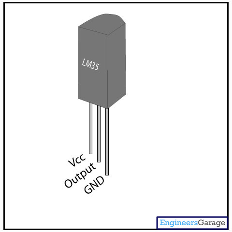
Lm35 Temperature Sensor:-

LM35 Temperature Sensor Image
LM35 is a precision IC temperature sensor with its output proportional to the temperature (in oC). The sensor circuitry is sealed and therefore it is not subjected to oxidation and other processes. With LM35, temperature can be measured more accurately than with a thermistor. It also possess low self heating and does not cause more than 0.1 oC temperature rise in still air.    
The operating temperature range is from -55°C to 150°C. The output voltage varies by 10mV in response to every oC rise/fall in ambient temperature, i.e., its scale factor is 0.01V/ oC.
Pin Diagram: 
LM35 Temperature Sensor pin diagram, PinOut
Pin Description: 

Pin No
Function
Name
1
Supply voltage; 5V (+35V to -2V)
Vcc
2
Output voltage (+6V to -1V)
Output
3
Ground (0V)
Ground

AT89C51 Microcontroller:-

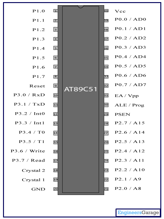
AT89C51 Microcontroller, Atmel 89C51 Controller Image
AT89C51 is an 8-bit microcontroller and belongs to Atmel's 8051 family. ATMEL 89C51 has 4KB of Flash programmable and erasable read only memory and 128 bytes of RAM. It can be erased and program to a maximum of 1000 times.
In 40 pin AT89C51, there are four ports designated as P1, P2, P3 and P0. All these ports are 8-bit bi-directional ports, i.e., they can be used as both input and output ports. Except P0 which needs external pull-ups, rest of the ports have internal pull-ups. When 1s are written to these port pins, they are pulled high by the internal pull-ups and can be used as inputs. These ports are also bit addressable and so their bits can also be accessed individually.
 
Port P0 and P2 are also used to provide low byte and high byte addresses, respectively, when connected to an external memory. Port 3 has multiplexed pins for special functions like serial communication, hardware interrupts, timer inputs and read/write operation from external memory. AT89C51 has an inbuilt UART for serial communication. It can be programmed to operate at different baud rates. Including two timers & hardware interrupts, it has a total of six interrupts.

Pin Diagram: 
AT89C51 Microcontroller Pin Diagram, Pinout
Pin Description: 

 Pin No
 Function
 Name
1
8 bit input/output port (P1) pins
P1.0
2
P1.1
3
P1.2
4
P1.3
5
P1.4
6
P1.5
7
P1.6
8
P1.7
9
Reset pin; Active high
Reset
10
Input (receiver) for serial communication
RxD
8 bit input/output port (P3) pins
P3.0
11
Output (transmitter) for serial communication
TxD
P3.1
12
External interrupt 1
Int0
P3.2
13
External interrupt 2
Int1
P3.3
14
Timer1 external input
T0
P3.4
15
Timer2 external input
T1
P3.5
16
Write to external data memory
Write
P3.6
17
Read from external data memory
Read
P3.7
18
Quartz crystal oscillator (up to 24 MHz)
Crystal 2
19
Crystal 1
20
Ground (0V)
Ground
21
8 bit input/output port (P2) pins
/
High-order address bits when interfacing with external memory
 
 P2.0/ A8
22
 P2.1/ A9
23
 P2.2/ A10
24
 P2.3/ A11
25
 P2.4/ A12
26
 P2.5/ A13
27
 P2.6/ A14
28
 P2.7/ A15
29
Program store enable; Read from external program memory
PSEN
30
Address Latch Enable
ALE
Program pulse input during Flash programming
Prog
31
External Access Enable;  Vcc for internal program executions
EA
Programming enable voltage; 12V (during Flash programming)
Vpp
32
8 bit input/output port (P0) pins
 
Low-order address bits when interfacing with external memory
 
 P0.7/ AD7
33
 P0.6/ AD6
34
 P0.5/ AD5
35
 P0.4/ AD4
36
 P0.3/ AD3
37
 P0.2/ AD2
38
 P0.1/ AD1
39
 P0.0/ AD0
40
Supply voltage; 5V (up to 6.6V)
Vcc


LCD:-


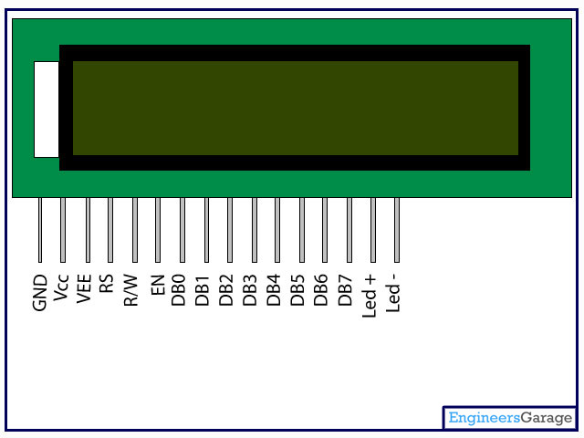
16 x 2 LCD | 16x2 Character LCD Module
LCD (Liquid Crystal Display) screen is an electronic display module and find a wide range of applications. A 16x2 LCD display is very basic module and is very commonly used in various devices and circuits. These modules are preferred over seven segments and other multi segment LEDs. The reasons being: LCDs are economical; easily programmable; have no limitation of displaying special & even custom characters (unlike in seven segments), animations and so on.
16x2 LCD means it can display 16 characters per line and there are 2 such lines. In this LCD each character is displayed in 5x7 pixel matrix. This LCD has two registers, namely, Command and Data.
The command register stores the command instructions given to the LCD. A command is an instruction given to LCD to do a predefined task like initializing it, clearing its screen, setting the cursor position, controlling display etc. The data register stores the data to be displayed on the LCD. The data is the ASCII value of the character to be displayed on the LCD.

Pin Diagram: 
16 x 2 LCD PinOut | 16x2 Character LCD Module Pin diagram
Pin Description: 
 Pin No
 Function
 Name
1
Ground (0V)
Ground
2
Supply voltage; 5V (4.7V – 5.3V)
 Vcc
3
Contrast adjustment; through a variable resistor
 VEE
4
Selects command register when low; and data register when high
Register Select
5
Low to write to the register; High to read from the register
Read/write
6
Sends data to data pins when a high to low pulse is given
Enable
7
8-bit data pins
DB0
8
DB1
9
DB2
10
DB3
11
DB4
12
DB5
13
DB6
14
DB7
15
Backlight VCC (5V)
Led+
16
Backlight Ground (0V)
Led-

ACD0804:-

ADC0804 | ADC 0804
Analog to digital converters find huge application as an intermediate device to convert the signals from analog to digital form. These digital signals are used for further processing by the digital processors. Various sensors like temperature, pressure, force etc. convert the physical characteristics into electrical signals that are analog in nature.

ADC0804 is a very commonly used 8-bit analog to digital convertor. It is a single channel IC, i.e., it can take only one analog signal as input. The digital outputs vary from 0 to a maximum of 255. The step size can be adjusted by setting the reference voltage at pin9. When this pin is not connected, the default reference voltage is the operating voltage, i.e., Vcc. The step size at 5V is 19.53mV (5V/255), i.e., for every 19.53mV rise in the analog input, the output varies by 1 unit. To set a particular voltage level as the reference value, this pin is connected to half the voltage. For example, to set a reference of 4V (Vref), pin9 is connected to 2V (Vref/2), thereby reducing the step size to 15.62mV (4V/255). 

ADC0804 needs a clock to operate. The time taken to convert the analog value to digital value is dependent on this clock source. An external clock can be given at the Clock IN pin. ADC 0804 also has an inbuilt clock which can be used in absence of external clock. A suitable RC circuit is connected between the Clock IN and Clock R pins to use the internal clock.
 
Pin Diagram: 
ADC0804 PinOut | ADC 0804 pin diagram
Pin Description: 

Pin No
Function
Name
1
Activates ADC; Active low
Chip select
2
Input pin; High to low pulse brings the data from internal registers to the output pins after conversion
Read
3
Input pin; Low to high pulse is given to start the conversion
Write
4
Clock Input pin; to give external clock.
Clock IN
5
Output pin; Goes low when conversion is complete
Interrupt
6
Analog non-inverting input
Vin(+)
7
Analog inverting Input; normally ground
Vin(-)
8
Ground(0V)
Analog Ground
9
Input pin; sets the reference voltage for analog input
Vref/2
10
Ground(0V)
Digital Ground
11
8 bit digital output pins
D7
12
D6
13
D5
14
D4
15
D3
16
D2
17
D1
18
D0
19
Used with Clock IN pin when internal clock source is used
Clock R
20
Supply voltage; 5V
Vcc


                                            SUMMARY

8051 Microcontroller (AT89C51) based Digital Thermometer Project

Fahrenheit scale digital thermometer is a temperature indicator which displays temperature in Fahrenheit scale. It is similar to Celsius scale digital thermometer, except a little modification in the microcontroller program. The temperature sensed in Celsius scale in the Celsius scale thermometer project is converted into the Fahrenheit scale temperature just by using the Celsius to Fahrenheit conversion formulae. This project also uses 8051 microcontroller (AT89C51).